History: In the early 1970s IBM invented CGA packages using plain Pb90/Sn10 solder columns, almost 10 years before Bell Laboratories introduced the solder ball for ceramic CBGA packages (Circa 1979-1980). In the early 1980s, Raychem improved solder columns by wrapping copper ribbon around Pb80/Sn20 solder core, with measurable improvements in operating life. In 1989 Motorola and Citizen jointly delveloped plastic BGA (PBGA) packages, originally named OMPAC (Over Molded Pad Array Carrier)
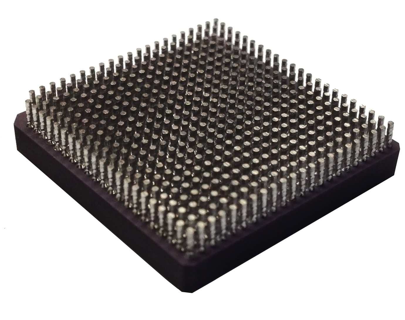
Older style solder columns are constructed of high melting temperature Pb90/Sn10 wire (or cast) without copper wrapping. Such "plain" columns tend to decrease electrical performance, especially at higher frequencies. Columns increase the overall package profile height, as compared to BGA components.
Solder columns are available in a variety of lengths from 1.0mm to 2.54mm. However, solder columns of 2.21mm nominal length tend to be the industry norm for most CCGA packages. Longer columns, such as 3.81mm, are useful for raising IC packages with bottom mounted decoupling capacitors off the circuit board.
Ideally, the diameter of the solder column should be roughly 75% of the landing pad diameter to allow a proper annular solder fillet to form around both ends of solder columns after joining the IC package to thePCB circuit board. Solder columns are available with diameters as small as Ø0.20mm and as large as Ø0.56mm (Ø0.89mm for certain applications).
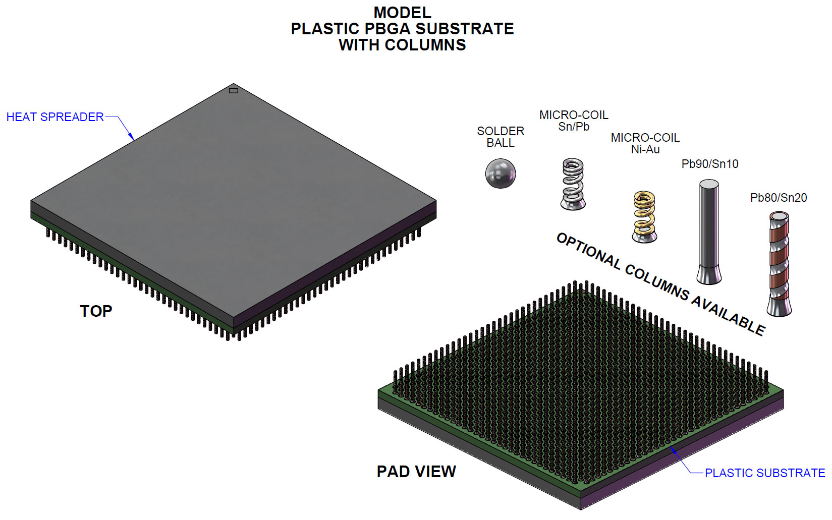
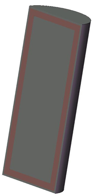
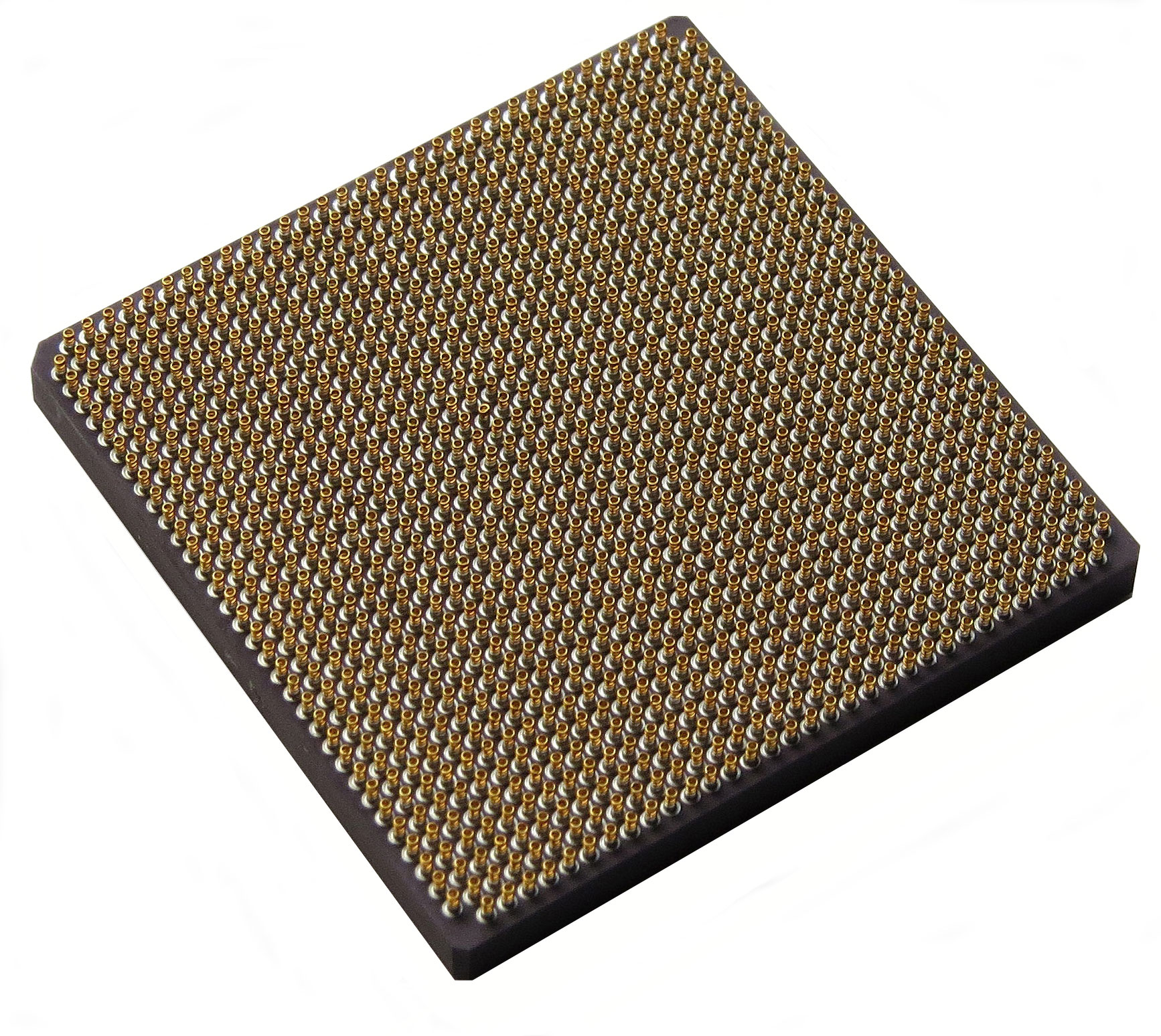
Solder columns have been successfully attached to organic PBGA substrates as illustrated in Figure 2. Ø0.50mm diameter solder columns tend to be the industry norm for 1.0mm and 1.27mm pitch ceramic IC packages. Smaller size solder columns with Ø0.38mm diameter are required for commercial off-the-shelf (COTS) 1.0mm pitch organic substrates (PBGA without solder balls), since most 1.0mm pitch PBGA packages have Ø0.50mm solder mask defined pads (SMD). Even smaller solder columns Ø0.25mm ~ 0.30mm diameter are required for 0.8mm pitch PBGA packages, depending on the diameter of the solder mask defined pads.
|
Solder columns are constructed of high melting point solder alloys. Solder Columns do not collapse during reflow to the PCB circuit board. Typically, Military/defense/aerospace applications require eutectic Sn63/Pb37 solder paste; however, commercial applications require SAC305 lead-free solder pastes.
At the time of this writing, high lead bearing solder columns such as Pb90/Sn10 and Pb85/Sn15 are exempt from RoHS per IPC-1752A 7(a) published March 2011.
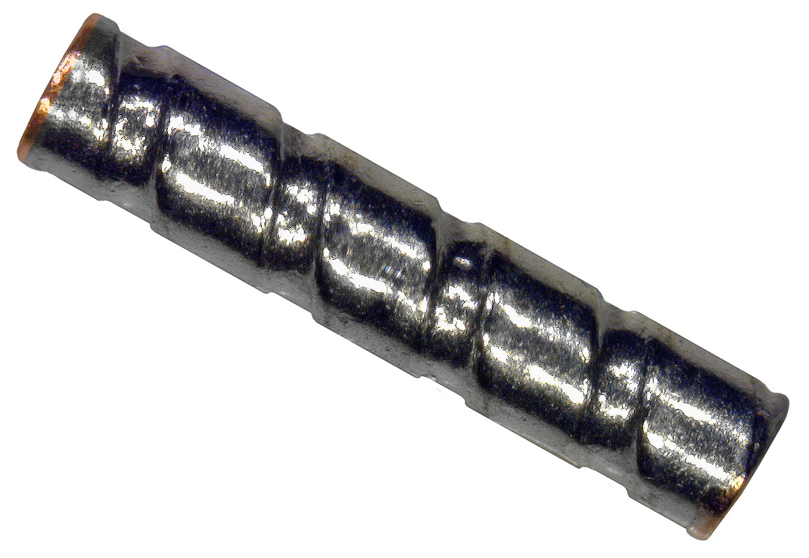
Solder columns are constructed of high melting temperature alloys, including Pb80/Sn20 or Pb90/Sn10, wound with an outer layer of oxygen free (OFHC-101 or alloy CDA101) copper. The thin layer of copper ribbon (0.025mm to 0.038mm thick) is spirally wrapped around the column. Columns are coated with eutectic Sn63/Pb37 to cover the copper ribbon and form a lap joint between the copper to the solder column as shown in Figure 3
 |
Click Enlarge
Fig 3. Copper Wrap Solder Column
Pb80/Sn20 Standard and New and Pb90/Sn10 Copper Wrap |
|
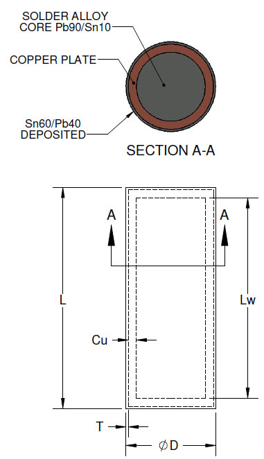
Pb90/Sn10 solder columns constructed with electroplated Cu copper shield provides 30% lower thermal resistance than copper wrapped columns to conduct heat away from the bottom of the IC package to the ground-plane of the circuit board as illustrated in Figure 4. The thickness of the Cu copper is 0.025mm to 0.050mm. A thin coating of Sn60/Sn40 covers the exterior Cu copper.
|
 |
|
 |
Click Enlarge
Fig 4. Section View Pb90/Sn10 Electroplated Cu
Coated with Sn60/Pb40 |
|
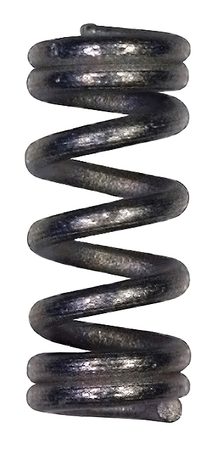
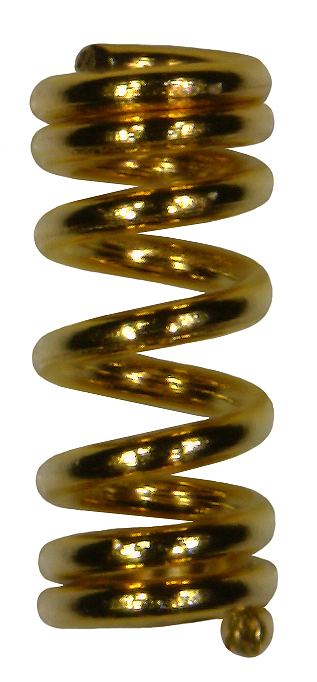
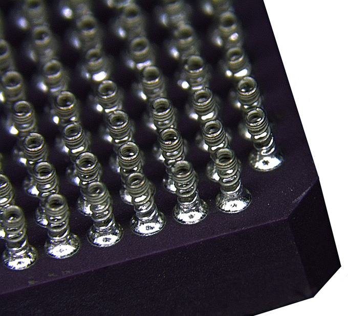
Micro-Coil Springs, introduced by NASA, provide an alternative to traditional solder columns. The base material is Beryllium-Copper (Be-Cu) wire. The wire is electroplated with a choice of Pb60/Sn40 or Ni-Au, shown in Figure 5 The NiAu gold (Au 2.5µm maximum) plated version provides a lead-free solution when combined with SAC305 fillets.
Coil size is Ø0.50mm (O.D.) diameter by 1.27mm long (free-load length) is use with 1.0mm pitch ceramic IC packages with Ø0.80mm pads. A smaller coil with Ø0.40mm (O.D.) diameter and 1.0mm length is used when attaching to organic PBGA substrates with Ø0.50mm solder mask defined pads.
|
 |
|
 |
Click Enlarge
Fig 5. NASA Micro-Coil Spring. SnPb plated and NiAu Gold Plated |
|
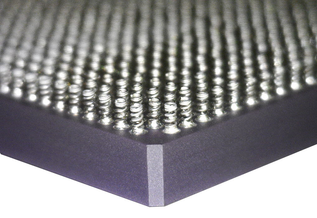
Figure 6 shows are examples of NiAu Gold plated Micro-Coil Springs (lead-free solution) attached to a ceramic CCGA with SAC305 fillets.
|
 |
|
 |
Click Enlarge
Fig 6. NiAu Gold Micro-Coil Spring attached to Ceramic CCGA1152 |
|
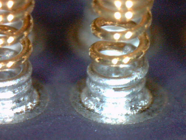
Figure 7 shows are examples of SnPb plated Micro-Coil Springs attached to a ceramic CCGA with eutectic Sn63/Pb37 fillets.
|
 |
|
 |
Click Enlarge
Fig 7. SnPb plated Micro-Coil Spring attached to Ceramic CCGA1152
Eutectic Sn63/Pb37 solder paste |
|
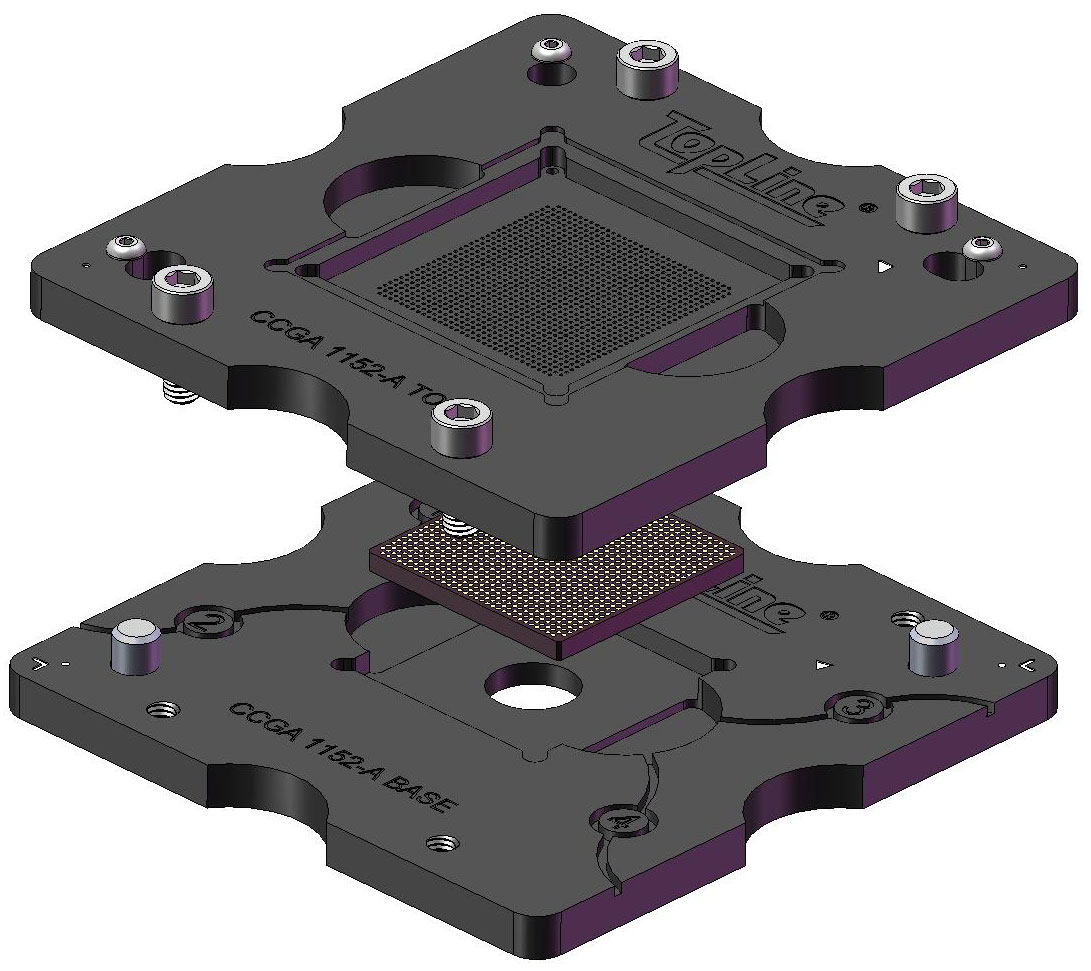
Graphite tool-sets are required to attach solder columns to CCGA packages. The tool-sets are designed for specific size, pad counts and ceramic and organic PBGA style Land Grid Array (LGA) substrates. The tool-set includes a bottom graphite to hold the LGA substrate and a mating top graphite to align Flip-PackTM cassettes pre-loaded with columns. Use a pallet to hold the bottom graphite during solder paste stencil printing. An entry level tool-set can process volumes up to 500 CCGA packages per month. You can increase throughput by adding more bottom graphite bases and top graphite tools to 10,000 packages per month. Refer to CCGA Tooling for more details. Aslo refer to CCGA Flip-Pack for more details on cassette carriers that are pre-loaded with solder columns or Micro-Coil Springs.
Figure 8 shows an example of a typical Graphite tool-set.
|
 |
Click Enlarge
Fig 8. Graphite Tool-Set for Attaching Columns to CCGA Package |
TopLine manufactures a wide range of CCGA - Column Grid Array packages with internal Daisy Chain circuitry. Daisy Chain provides engineers with a simple tool to learn valuable information about causes of failures.
Research starts by mounting Daisy Chain devices onto a test vehicle board with complimentary daisy chain circuitry. This combination creates a short circuit with near zero ohms resistance measured at test points on the test vehicle board. The test vehicle board is subjected to harsh environmental conditions, such as dropping, vibrating, freezing and heating until a connection breaks.
The onset of failure is measured after the Daisy Chain resistance changes by more than 20%, and eventually becomes an open circuit (∞ ohms) with full failure. The failure can be observed and measured with an ohm-meter with DC voltage applied.
You can make improvements in the assembly process using analysis and experimentation with Daisy Chain circuits.
Simplified Daisy Chain Circuit ia shown in Figure 9.
|
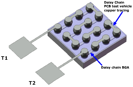 |
Fig. 9 "Failure" occurs at onset of 20% change in resistance
or when an open circuit is measured (∞ Ω) between T1 ~ T2. |
| |
| Contact TopLine for assistance with CCGA packages and solder columns. |
|
CCGA PDF Catalog
•
Home
|
 |
TopLine Corporation
95 Highway 22 W
Milledgeville, GA 31061, USA
Toll Free USA/Canada (800) 776-9888
International: 1-478-451-5000
Email: sales@topline.tv
|
|